 18922924269
 CO., LTD")
Introduction of High-power Pulsed Magnetron Sputtering Technology (Part 2)
Characteristics of high ionization plasma deposition film:
In magnetron sputtering technology, the energy transferred to the film-forming particles can be controlled by controlling the change of deposition parameters, so as to regulate the film properties 28. Among the various methods of providing energy for growing films, bombardment with ionized material has been widely used 29,30. Many studies have shown that the plasmonic film interface is influenced by the energy of the bombarded ions, the flux, their properties, and the Angle of incidence during film growth 31,32. In HiPIMS, high pulsed ion fluxes can be obtained at the substrate. These parameters determine the efficiency with which momentum is transferred to the atoms of the film 33 and have an impact on the microstructure 31 as well as mechanical, optical and electrical properties of the film 34-36.
1. Deposit on a complex shape substrate
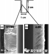
The deposition of uniform thin films on substrates of complex geometry is a requirement for many technological applications, such as metallization of submicron patterns in optical and semiconductor devices 37,38 and the deposition of thick protective layers on forming tools and turbine blades 39,40. In conventional sputtering techniques such as DCMS, deposition fluxes are highly anisotropic, resulting in uneven deposition, porosity, and poor coverage at substrate locations along the low-flux direction. To alleviate these problems, highly ionized deposition fluxes can be used, since the trajectory of charged material can be controlled by electric and magnetic fields, as shown in FIG. 2.
Figure 2. Cross-sectional scanning electron microscopy (SEM) images of Ta films grown by (a) HiPIMS and (b) DCMS on Si substrates fixed to one side of a trench with a depth of 2 cm and an area of 1 cm2. The films deposited by HiPIMS are dense and columnar crystals grow perpendicular to the Ta/Si interface. The films deposited by DCMS have a porous microstructure with columnar crystals tilted toward the flux direction 11.
2. Phase composition of HiPIMS regulation
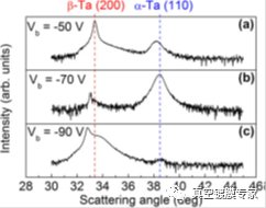
The phase composition of a film is crucial for its mechanical, electrical and optical properties. During sputtering, relatively low growth temperatures and high deposition rates can limit kinetic growth 41. This, in combination with the extremely high cooling rate (1013 ks-1) during condensation of the steam on the substrate, results in non-equilibrium growth. Changes in thermodynamic and kinetic conditions during deposition make possible changes in phase composition. Numerous studies have shown that high-energy ions can be used for this purpose, as they can trigger surface and volume diffusion processes, induce changes in film structure and chemical composition 42, and cause the generation of internal stresses. This is shown in Figure 3.
FIG. 3. X-ray diffraction patterns of Ta thin films deposited with HiPIMS on Si substrates at different bias (a) 50, (b) 70 and (c) 90 V, induced compressive stress to generate α-TA8 under -70V bias ion bombardment.
3. Thin film microstructure control and interface engineering
Deposition using state of the art sputtering techniques at relatively low temperatures, typically below 0.4Tm, where Tm is the melting temperature of the deposited material, can only activate surface diffusion leading to the formation of thin films with columnar microstructure and intercolumnar pores. Figure 4 (a). Films grown using HiPIMS are characterized by high ion fluxes to the substrate (up to a few hundred milliamps per square centimeter) and relatively low energy. These growth conditions enhance surface diffusion and lead to film densification 46,47, as shown in FIG. 4(b). On substrates that increase the available ion fluxes (e.g., by increasing peak target currents), re-nucleation 46,48 results in inhibition of columnar structures and transition from dense polycrystalline globules to nanocrystal microstructures 49. See FIG. 4(c) -4 (d). When high energy flux cannot be obtained during growth, the spherical microstructure is the result of impurity phase segregation, which hinders the growth of crystals and grains. Therefore, it is clear that low-energy and high-throughput ion irradiation in HiPIMS process can be used to overcome the characteristics of low density and rough microstructure, and obtain the unique morphology of low-temperature sputtering deposition compared with DCMS deposition films, which makes the films have higher hardness 48,50 and lower friction coefficient 9,51. And improves scratch, wear and corrosion resistance.
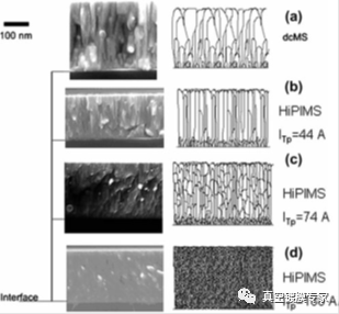
Figure 4 :(a) the cross-sectional SEM image of CrN film deposited on Si by DCMS, and the peak target currents of HiPIMS were (b) 44 a (1.0 a cm-2), (c) 74 a (1.7 a cm-2), and (d) 180 a (4.0 a cm-2). The graph below. The increase of the peak target current results in the transformation of the dense polycrystalline form to the featureless nanocrystalline form. The sketch next to each SEM image is only for the reader's convenience as a schematic 11.