 18922924269
 CO., LTD")

Ceramic metallization solutions
Ceramic metallization solutions
Technical features:
1. AEGD ion source cleaning + HiPIMS technology to prepare Nb2O5, SiO2, etc., and the film base has high adhesion.
3. HiPIMS+DC composite technology, reactive sputtering is not poisoned, and the process window is wide.
4. HiPIMS technology has high ionization rate, dense film layer and high refractive index. The refractive index of Si3N4 is as high as 2.17.
Technical advantages
1. High bonding strength
The traditional ceramic substrate needs to be plated with Cr, Ti, W and other primers to enhance the bonding force with the ceramic substrate. According to specific requirements, the direct copper plating technology on the surface of the ceramic substrate is developed, which can meet the requirements of high bonding force. The copper film is peeled off from the ceramic substrate in the pull-out test, and the maximum bonding force reaches 115N/mm2.

2. High density
The customized high-energy pulsed composite plasma power source and the optimized plasma source can prepare the Cu film with dense morphology, no obvious grain boundary holes and other defects in the cross section, and the high-density copper film has high bonding force, and can prepare ultra-thick copper film.
Customized high-energy pulsed composite plasma power supply with optimized plasma source

3. High surface flatness
The special substrate surface activation technology damages the roughness of the ceramic substrate. During the deposition process, the ion-to-atomic ratio is flexibly adjusted, and a high-flatness film surface can be obtained, and the surface roughness can reach Ra=0.025um.
Special Substrate Surface Activation Technology Department Damaged Ceramic Substrate

4. Heat resistance and oxidation resistance and welding performance
After the ceramic metallization, the copper film is directly soldered at 400°C. After the soldering is completed, the tin liquid is melted, and the soldering surface is smooth and smooth without any bubbles. After soldering at 395 °C, the tin rate can be guaranteed to be above 95%, and the bonding strength can be maintained without degradation.
Heat and oxidation resistance and solderability

5. Micro-deep hole coverage capability

4. Application
It is applied to high-end ceramic/glass packaging substrates to achieve special application requirements such as high thermal conductivity, high operating frequency, operating temperature, and high bonding strength. At the same time, the complex 3D structure of packaging substrates and micro-deep holes can be uniformly covered; optical fiber metallization to achieve aerospace grade High sealing performance, high bonding strength, high and low temperature and other application scenarios; metallization of ceramic substrates such as ferrite and magnesium titanate to achieve high welding performance, high frequency signal transmission and other applications.SEM in micropores
Inner hole DLC coating
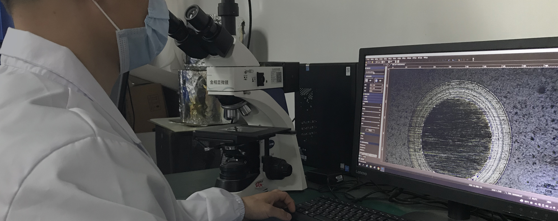
Ceramic copper plated section
Ceramic micro deep hole metallization
Ceramic coating
Ceramic DLC coating

Micropore SEM electron microscope

Inner hole DLC coating
Application examples of ceramic metallized coating:

Ceramic copper-plated section

Microdeep hole metallization of ceramics

Ceramic product coating

Large area ceramic DLC coating